CNC Semiconductor Manufacturing for Ultra-Precise, Micro-Scale Components
- All uploads are secure and confidential
We Help From Prototyping to Production
Prototyping
Engineering Validation and Testing
Production Validation and Testing
Mass Production
Top Proto produces precision-machined components for a broad range of semiconductor equipment and process systems:
- Wafer chuck bodies, electrostatic chuck base plates, and wafer carrier precision components
- Process chamber components in aluminum, stainless steel, and quartz-compatible materials
- Robotic end effector blades and wafer transfer arm structural components for cleanroom automation
- Precision lens mounts, stage components, and optical alignment fixtures for lithography and inspection systems
- Vacuum sealing surfaces, O-ring groove profiles, and gas delivery manifold components
- Ion implant equipment components requiring non-magnetic materials and controlled outgassing
- CMP (Chemical Mechanical Planarization) equipment components including carrier heads and platen components
- Metrology fixture components, probe card frames, and wafer inspection stage parts
- Quartz tube holders, ceramic component interfaces, and high-temperature process equipment structural parts
• Cleanroom automation fixture components, SMIF pod interfaces, and FOUP handling guide assemblies
Our Services
Additive manufacturing for semiconductor equipment design validation models, non-critical enclosure components, and tooling aids that do not require cleanroom surface conditions.
Why Top Proto for Semiconductor Manufacturing?
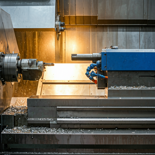
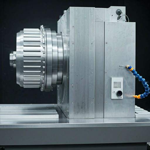
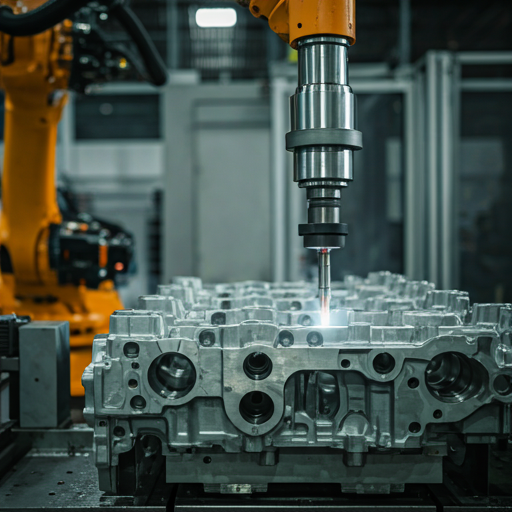
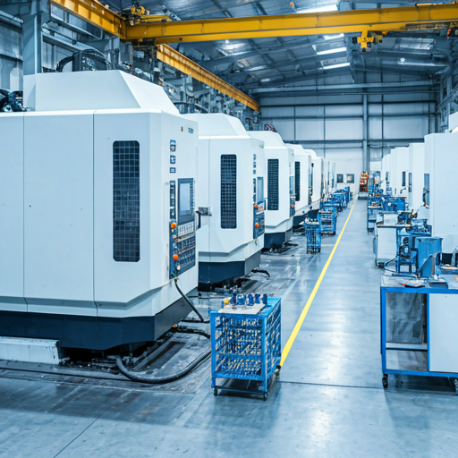
Ultra-Precision Machining Capability
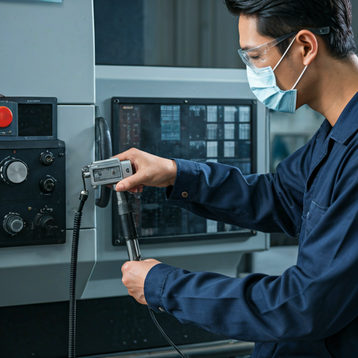
Top Proto achieves dimensional tolerances down to +/-0.003mm on critical semiconductor equipment features using precision-calibrated 5-axis machining centers with temperature-controlled work environments. Positional accuracy between features is verified by CMM measurement with inspection uncertainty documented in the part report.
Cleanroom-Compatible Surface Treatment and Packaging
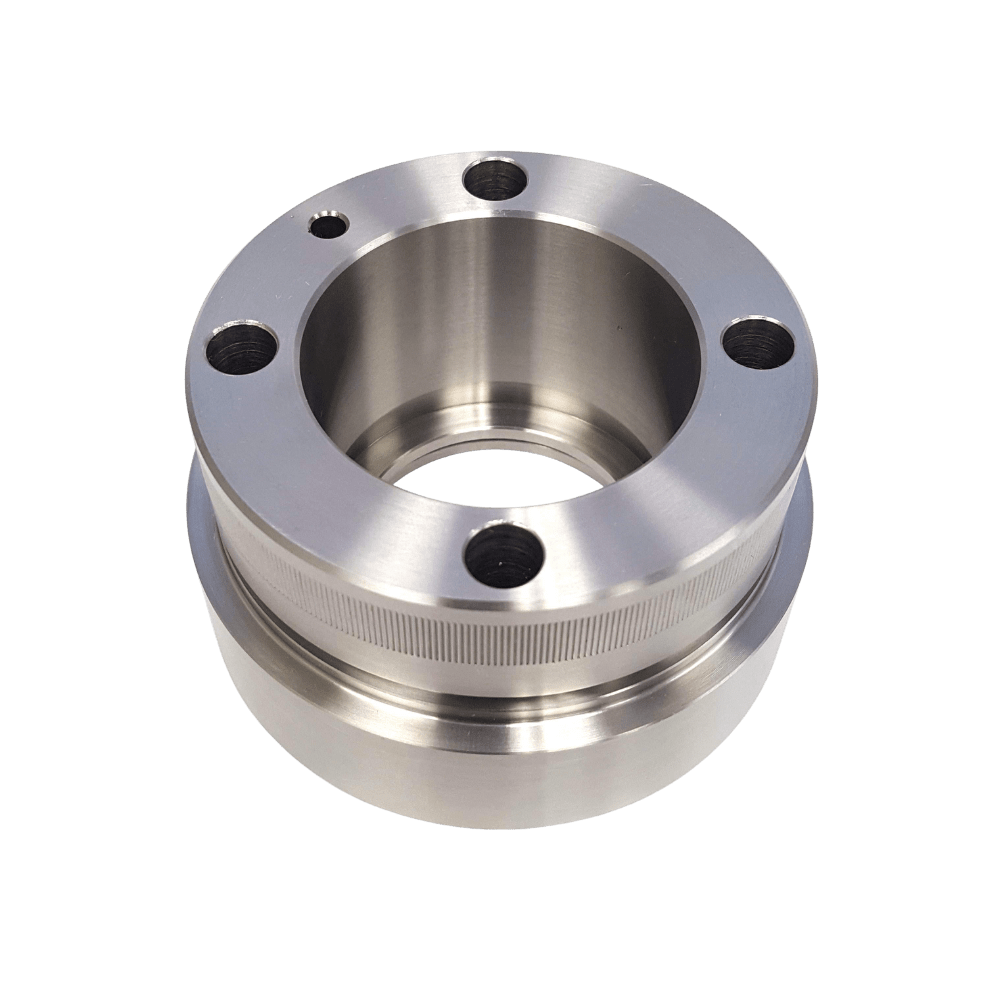
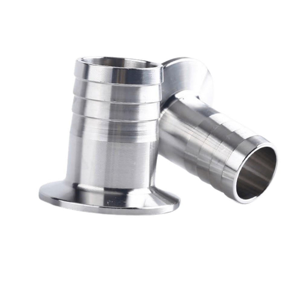
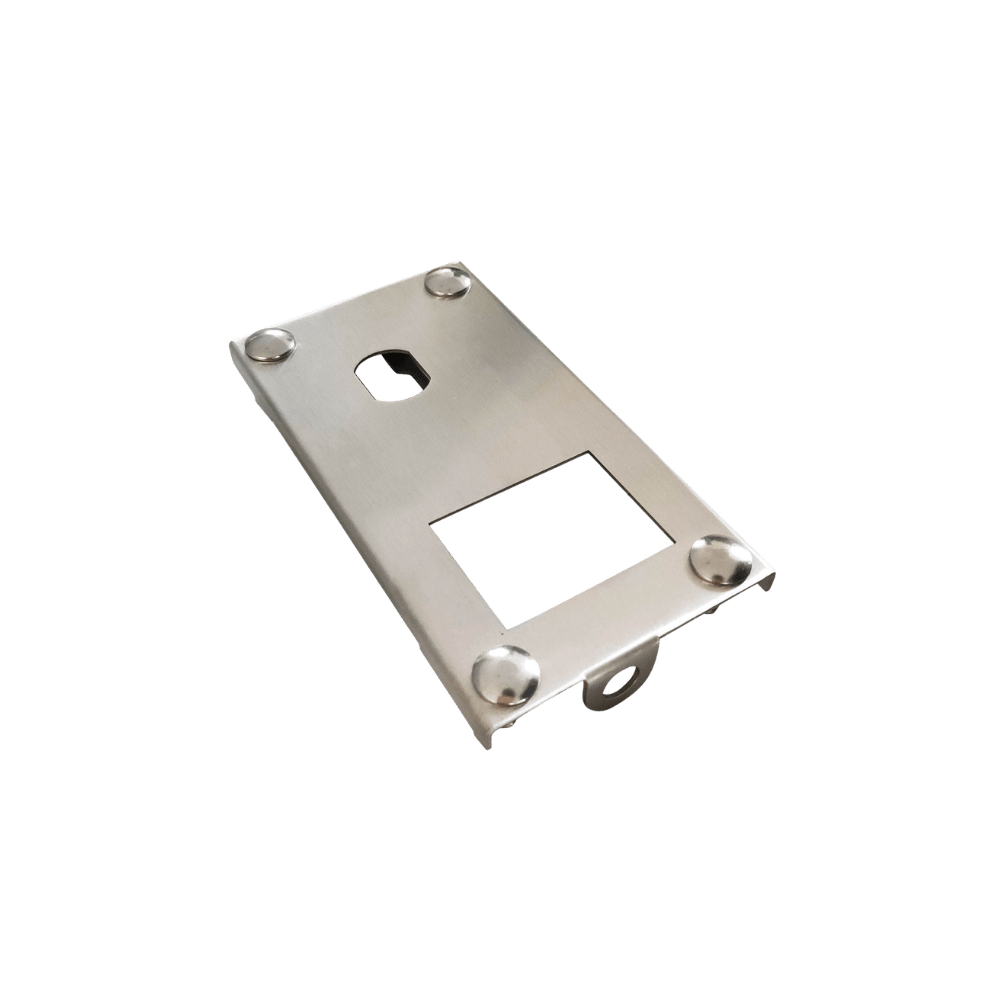
Semiconductor components at Top Proto are degreased, inspected under UV light for contamination, and packaged in double-sealed cleanroom bags before boxing. Electropolished stainless steel surfaces achieve Ra 0.1 or below, meeting vacuum equipment cleanliness requirements. Surface cleanliness documentation is provided on request.
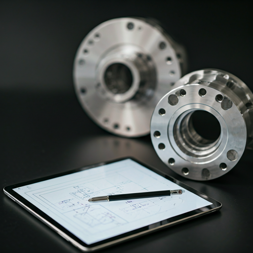
Invar and Non-Magnetic Material Expertise
Semiconductor optical and lithography equipment requires components with minimal thermal expansion (Invar 36) and non-magnetic properties (titanium, austenitic stainless steel) to maintain positional stability during operation. Top Proto machines these materials with the parameter selection and tooling choices appropriate for their specific machining characteristics.
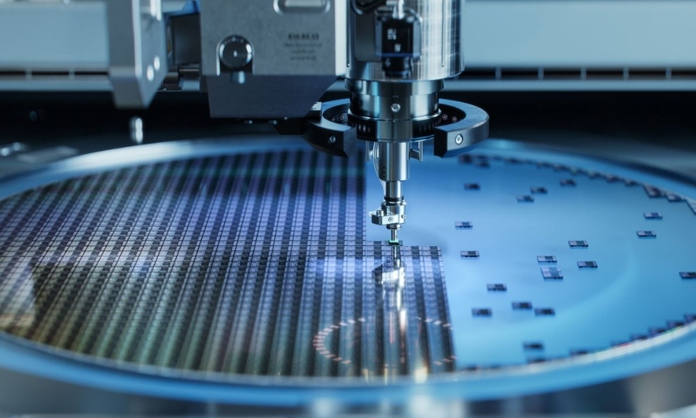
Vacuum Compatibility and Outgassing Control
Semiconductor process equipment components must meet vacuum compatibility requirements covering surface finish, material outgassing, and absence of contaminants. Top Proto applies electropolishing and passivation treatments aligned with vacuum compatibility specifications, and avoids machining lubricants and cutting fluids that introduce high-outgassing surface residues.
Materials and Surface Finishes for Semiconductor Parts
Surface Finishes
Manufacture Through Latest Technology
End To End Solutions
How We Works – 3-Stages Workflow
We guarantee that CNC parts are delivered on time and that the process is completely transparent in the following 3 simple steps:
Upload Your Files
Instant prices with DFM feedback for many file types.
We Manufacture Your Parts
You can select from many materials and methods.
Tracking and Receiving Your Parts
View the QC documentation and inspection photographs.
Frequently asked questions
What dimensional tolerances can you achieve for semiconductor equipment parts?
Top Proto achieves tolerances down to +/-0.003mm on critical features for semiconductor equipment components using precision 5-axis machining centers. Flatness on wafer chuck and process chamber sealing surfaces is held to 0.005mm or better depending on part geometry. All critical dimensions are verified by CMM measurement with uncertainty documented in the inspection report.
Can you machine invar and other low-expansion alloys?
Yes. Top Proto machines Invar 36 and other controlled-expansion alloys for semiconductor optical mounting structures, reference fixtures, and precision alignment components. Invar machining requires specific cutting parameter selection to minimize work hardening and achieve the required surface finish without inducing residual stress.
Do you provide cleanroom-compatible packaging?
Yes. Top Proto provides cleanroom-compatible packaging as standard for semiconductor equipment components. Parts are degreased, inspected for contamination, and double-bagged in cleanroom-grade polyethylene bags before boxing. Additional packaging specifications including nitrogen purging and moisture indicator inclusion are available on request.
Can you machine vacuum-compatible components for semiconductor process chambers?
Yes. Top Proto produces vacuum-compatible components in electropolished 316L stainless steel and Type II or hard anodized aluminum for semiconductor process chamber applications. O-ring groove geometry, vacuum flange face flatness, and surface roughness are inspected and documented. Outgassing-compatible machining practices are applied throughout the production process.
What surface finishes are available for semiconductor equipment parts?
Top Proto applies electropolishing to stainless steel components achieving Ra 0.1 or below, passivation to ASTM A967, Type II and hard anodizing for aluminum process chamber components, precision bead blasting for controlled surface texture, and cleanroom degreasing as standard finishing for semiconductor equipment orders.